Skip to content
Menu
Japanese
CHINESE
HOME
Products
Product Lineup
Exposure system for experimentation and research
Exposure system for compound semiconductor (mask aligner)
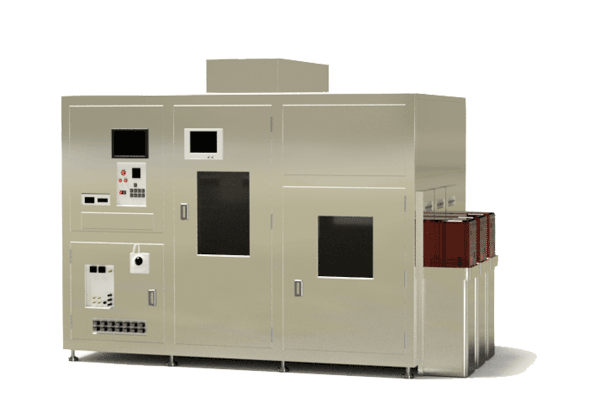
Exposure machine for Ø200mm and Ø300mm
Ø200mm compatible exposure equipment
Ø300mm compatible exposure equipment
Maskless exposure system
Exposure system for MEMS
Exposure system for films
Exposure system for FPDs
Proximity exposure system for G1~G4.5 substrates
Vertical proximity exposure system for G3~G5 substrates
Vertical exposure system for supersize
Exposure system for other mass production
Substrate Encapsulatie system
Desktop Mask Aligner
About us
Message from Management
Company Profile
Company Landmarks
Office/Factory Maps
Head Office Map
Eastern Factory・ Second Eastern Factory Map
Oharano factory Map
Yokoohji factory Map
Tokyo Office Map
Main facilities
Production System
Engineering
Production
Maintenance
Technologies
Technologies
Optomechatronics
Ideal collimated light
Structure of lamp housings
LCD color filter production processes
The “Moving UV mask” method
Maskless exposure technique
Contact us
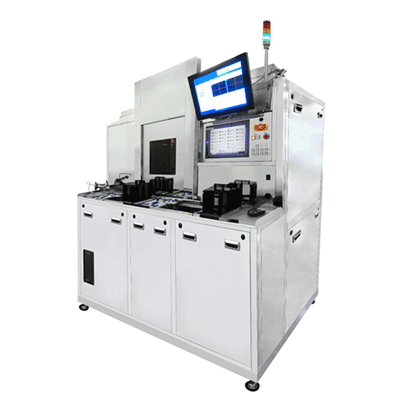
Exposure machine for Ø200mm and Ø300mm
Products
Exposure machine for Ø200mm and Ø300mm
Exposure machine for Ø200mm
Exposure machine for Ø300mm