

Directly drowning a pattern image on a substrate plate is possible by employing their original high speed imaging method “Point Array”.
Main feature
- Direct imaging exposure is applicable to experimentation, research, prototype, small-lot production, or etc.
- Applicaple to products such as semiconductors, electronic components, screen mask, metal mask, high-end PCB, high-density packaging, MEMS and FPDs.
- No photomask is needed in the lithography process, which minimizes development cost and time lag to the market.
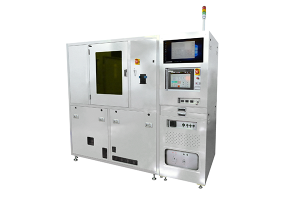
- Also, custom system composition is available to meet the customers’ requests.
Main spec
| Type | MX-1201 | MX-1201E | MX-1205 | ||||||
|---|---|---|---|---|---|---|---|---|---|
| One engine | Two engines | ||||||||
| Minimum line width (※1) | [μm] | 5 | 3 | 2 | 1 | ||||
| Data resolution | [μm] | 0.488 | 0.25 | 0.1 | 0.05 | ||||
| Maximum substrate size | [mm] | 200 x 200 | 200 x 200 | 100 x 100 | |||||
| Effective exposure area | [mm] | 200 x 200 | 200 x 200 | 100 x 100 | |||||
| Peak wave length | [nm] | 405 | 375 | 405 + 375 | 375 | 405 | 375 | 375 | |
| Scanning speed | [mm/s] | 43.94 | 22.5 | 9 | 4.5 | ||||
| Tact time (※2) | [s,min] | 180 [s] | 145 [s] | 320 [s] | 16 [min] | 27 [min] | |||
| Maximum exposure dose (※3) | [mJ/c㎡] | 245 | 70 | 245 + 70 | 70 | 460 | 135 | 50 | 100 |
※1 Value varies according to the conditions (Ex. photo-resist,film thickness, and development conditions)
※2 The alignment time is excluded.
※3 Under the maximum scanning speed.