

A mask moves during (UV) radiation and controls the energy incident on the photoresist surface, thereby enabling fabrication of 3D microstructures with arbitrary curve or slope.
Main feature
- Our original mirror & lens optical system realizes uniform radiation covering the full exposure area.
- Equipped with gap sensors for non-contact gap making with a good in-plane uniformity, and an alignment system composed of microscopes and a XYθstage for aligning the existing layer(s) on a substrate to a mask pattern.
- In the “Moving UV mask” method (in which a piezo stage micropositions a mask during exposure), the thick resist’s sidewall slope angle is controllable, thereby fabricating 3D microstructures is possible.
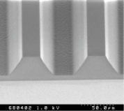
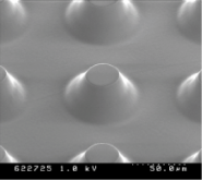
Example of 50μ-thick resist pattern
L/S=50μm
Mask travel =20μm
Dot=Φ50μm
Mask travel =Φ25μm

Main spec
| MUMseries | ||
|---|---|---|
| Mask size | Max 9″ x 9″ x t3.0 mm | |
| Substrate size | Max Φ8″(Wafer) | |
| Light source | Super high-pressure mercury lamp:500W or 1kW | |
| Outer dimensions and weights | Main body dimensions | W2120 x D1305 x H1850 mm |
| Main body weight | 640kg | |
※Custom substrate size, mercury lamp wattage or other special spec available.