

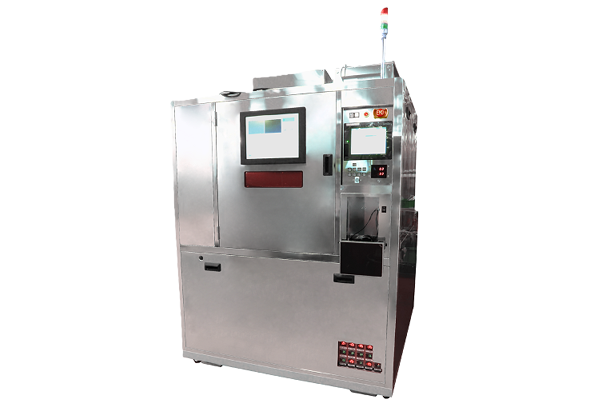
Exposure system that prints patterns on photoresist-coated substrates aligned with a mask, in which an automatic alignment mechanism is available for multi-layer exposure. Substrate loading, alignment, exposure, and unloading are performed automatically.
Main feature
- Our original parallelization mechanism enables making a proximity gap between a mask and a wafer with high accuracy.
- Our original high speed image processing technique realizes high accuracy alignment.
- The image processing technique can enable propositioning a thin, warped or fragile wafer such as quartz (optional).
- Our original precision contact-pressure control mechanism enables a wafer to contact a mask with high accuracy.
- A vacuum chuck is employed to fix a wafer on its back side, realizing high speed & accuracy and stable automatic transfer of the wafer.
Main spec
| MA-4000 | |||
|---|---|---|---|
| Wafer size | Ø2~4″ | Ø4~6″ | |
| Mask size | □5″ | □7″ | |
| Light source | Super high-pressure mercury lamp:500W or 1kW | ||
| Outer dimensions and weights | Main body dimensions | W1340 x D1430 x H1900mm | |
| Main body weight | 1120kg | ||
| Optional items | Production management system (D-Net), bottom-viewed auto alignment, ○/□ substrate compatibility | ||
※Custom substrate size, mercury lamp wattage or other special spec available.